March 1, 2021 feature
Nanoshape imprint lithography using molecular dynamics of polymer crosslinking
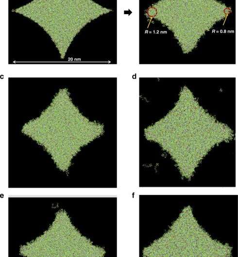
Nanoscale applications in energy, optics and medicine have enhanced performance with nano-shaped structures. Such architectures can be fabricated at high-throughput beyond the capabilities of advanced optical lithography. In a new report on Microsystems & Nanoengineering, Anushman Cherala and a research team at the University of Texas at Austin Texas, U.S., expanded on nanoimprint lithography and extended the previous simulation framework to improve shape retention by varying the resist formula and introducing new bridge structures during nanoshape imprinting. The simulation study demonstrated viable approaches for nanoshaped imprinting with good shape retention matched by experimental data.
Using a diamondlike nanoshape to form a half-pitch dynamic random-access memory (DRAM) node and understanding crosslinking in nanoshaped structures
In this work, the research team developed an atomistic model to study the shape retention of resist formulations used for nanofabrication techniques. Applications across energy storage, nanoscale photonics, multibit magnetic memory and bionanoparticles require high-throughput patterning and complex shape control at the nanoscale. Optical lithography is a key nanofabrication technique, where higher-resolution, large-area patterns can be formed by complementing photolithography with self-aligned double-patterning techniques alongside multiple lithography etch steps. Imprinting lithography including jet and flash imprint lithography can allow large-area patterning at sub-nanometer half-pitch with potential to pattern lithographic structures, including semiconductor devices and hard disks. Crosslinked resist materials can be used in such techniques under ultraviolet (UV) radiation. Using simulations of resist relaxation after UV crosslinking and template separation, materials scientists identified resist properties at the nanoscale as a limitation for shape retention.
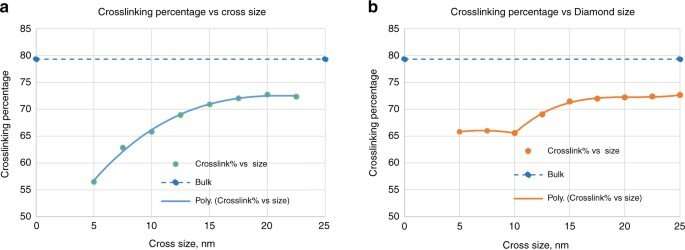
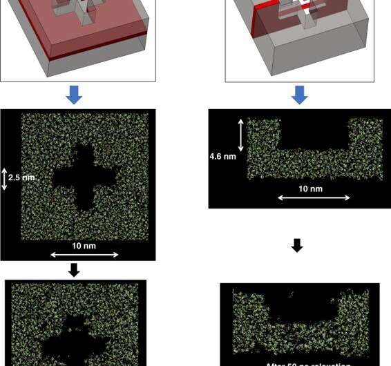
Scientists can employ a variety of techniques to improve shape retention in nanostructures including etch compensation and the addition of sub-resolution features. To investigate corner behavior of nanoshaped structures, Cherala et al. therefore prepared five unique 20-nm diamond structures. The constructs represented a half-pitch dynamic random-access memory (DRAM) deep trench capacitor design. The resist crosslinking quality influenced the material modulus and strength in the resist across the nanoshape. The team used molecular dynamics to estimate the quality and uniformity of crosslinking as a function of the shape and size of the feature. They then calculated the crosslinking percentage based on the number of carbon atoms with newly formed single bonds after crosslinking. As the nanoshape size reduced, the crosslinking quality degraded and did not reach the bulk crosslinking value.
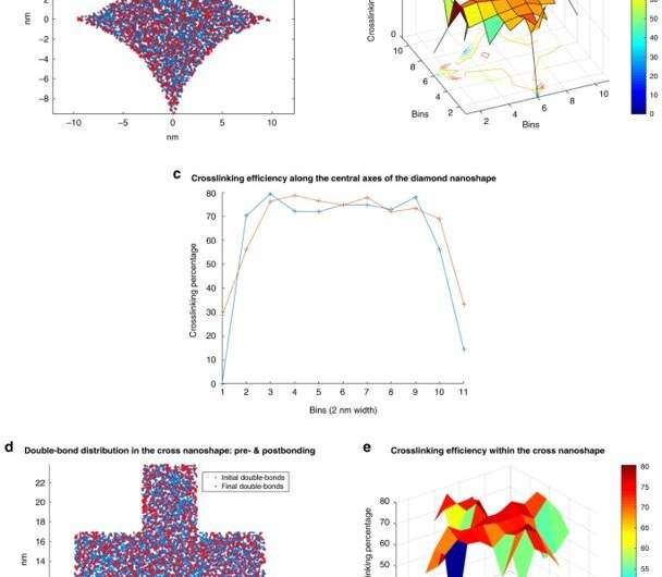
Bonding efficiency relative to the nanoshape structure and the computational design of resist for nanoshape structures
Crosslinking strongly depended on the location within the nanoshape of interest. Using the diamond structure, Cherala et al. showed similar levels of crosslinking to that of the bulk with sharply degraded corners. Based on the information of this crosslinking percentage, the team predicted shapes that are difficult to achieve. They then studied the composition of the imprint resist and used a molecular dynamic (MD) framework to understand the resists formulation itself. The resist formulation consisted of three acrylate monomer molecules including hexyl acrylate, isobornyl acrylate, and ethylene glycol diacrylate as the crosslinker. The team noted a correlation between the proportion of the crosslinker in the resist and the crosslinking percentage. Higher crosslinker amounts in the setup led to faster crosslinking, the process could also reduce the crosslinking percentage. The molecular dynamics design tool used in this work allowed the effective study of crosslinkers when forming cross and diamond nanoshaped structures. The team chose the cross nanoshape size and two resist formulations with 10 percent and 40 percent crosslinkers. Then they simulated crosslinking with each new resist formulation to analyze effects on the crosslinking percentage. Increased crosslinker density allowed improved bonding efficiency. This method can be repeated for each new nanoshape design consideration to retain nanoshapes.
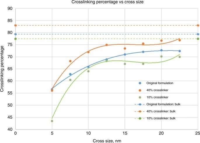
Improving shape retention using sacrificial structures and the effect of residual layer thicknesses
When developing a sharp corner at the nanoscale during diamond fabrication, researchers have often used reactive-ion etching-based design for nanoshape retention. Using sacrificial bridge structures, Cherala et al. showed how the existing bonding inefficiency could be overcome in the setup. In this way, Anushman Cherala and colleagues introduced improvements to the geometry of patterned nanostructures using sacrificial structures and enhanced resist formulations for improved shape retention. They performed molecular dynamics studies of crosslinking in nanoshapes as a function of size and shape to indicate how the extent of crosslinking decreased below a specific threshold size. For example, when the crosslinking percentage was specifically lower near the edges of nanoshapes, they used sacrificial bridges, to further improve shape retention. In this way, this work provides insights into nanoshape imprinting across sub-nanoscale half-pitch structures.
More information: Cherala A. et al. Extending the resolution limits of nanoshape imprint lithography using molecular dynamics of polymer crosslinking, Microsystems & Nanoengineering, doi.org/10.1038/s41378-020-00225-y
B. Stipe et al. Magnetic recording at 1.5 Pb m−2 using an integrated plasmonic antenna, Nature Photonics, doi.org/10.1038/nphoton.2010.90
Lam S. et al. Combating multidrug-resistant Gram-negative bacteria with structurally nanoengineered antimicrobial peptide polymers, Nature Microbiology, doi.org/10.1038/nmicrobiol.2016.162
Journal information: Nature Microbiology , Nature Photonics
© 2021 Science X Network


